
Thermal Simulation Is Moving Upstream. Are the Material Properties Keeping Up?
As semiconductor architectures become more three-dimensional, predictive thermal modeling depends on something that cannot be simulated away: reliable measurements of how materials and interfaces actually transport heat.
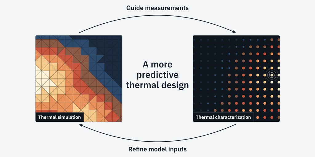
Semiconductor thermal simulation is becoming an increasingly important part of early-stage design. Once treated largely as a downstream verification activity, thermal analysis now influences decisions about device architecture, material selection, floor planning, and advanced packaging. This shift reflects a fundamental change in how modern semiconductor systems manage heat. Vertically stacked transistors, heterogeneous integration, chiplets, and three-dimensional memory architectures create increasingly complex thermal pathways. Heat must travel through multiple materials and interfaces whose properties may differ considerably from familiar bulk-material values.
Moving thermal simulation earlier in the design process is essential. But earlier simulation is only useful when the underlying material properties accurately represent the structures being designed.
Thermal Is Becoming a Design Input, Not Just a Signoff Requirement
In its article, Is it Getting Hot in Here? Why Thermal is No Longer a Signoff Problem, Keysight describes the growing interdependence of electrical, thermal, and mechanical behavior in advanced semiconductor systems.
As power densities increase and packaging becomes more complex, engineers can no longer evaluate these disciplines independently. Temperature affects electrical performance, thermal expansion creates mechanical stress, and packaging decisions influence the heat-removal pathways available to individual devices.
Keysight makes an important observation: “The answer is not simply more simulation.” Instead, the challenge is applying appropriate modeling fidelity throughout the design process, enabling engineers to identify thermal constraints while architectural decisions can still be changed. This is an important evolution. However, it introduces another question: What material properties should engineers use when those architectures have not yet been manufactured?
Traditional thermal simulations frequently rely on literature values, supplier specifications, or measurements performed on bulk materials. These inputs can be appropriate for certain applications, but may not capture the behavior of nanometer-scale films, multilayer structures, or interfaces produced by specific manufacturing processes.
The challenge is not simply to simulate earlier. It is to ensure that the physical assumptions underlying those simulations remain valid.
As Devices Become Three-Dimensional, Heat Takes More Complicated Paths
Two recent research papers illustrate why this distinction matters. In Beyond HBM-on-GPU: Thermal Design Envelope for 3D Volumetric DRAM-on-GPU Integration, researchers examine the thermal feasibility of integrating vertically oriented DRAM structures above GPUs. Their package-level modeling investigates how stack geometry, cooling-cavity conductivity, material placement, and power distribution affect thermal behavior. One finding is particularly revealing: stack height emerges as the dominant limitation on peak temperature, while the thermal conductivity of cooling cavities influences which configurations remain thermally feasible. This demonstrates that thermal constraints cannot always be addressed by improving external cooling alone. They are increasingly embedded in the physical architecture itself.
A related problem appears at the transistor level. In Self-Heating and Parasitic Effects in Multi-Tier CFET Design, researchers examine the consequences of vertically stacking multiple nanosheet transistors. Using technology computer-aided design (TCAD) models calibrated against experimental measurements, they compare two-tier and four-tier complementary field-effect transistor (CFET) structures. Their simulations indicate that upper-tier transistors experience greater self-heating as their distance from the substrate heat sink increases. For example, the modeled maximum temperature rise for the upper-tier pFET reaches 98.5 K in the four-tier configuration, compared with 74 K in the two-tier configuration.
These are simulated results for the studied structures, not universal temperature predictions for CFET devices. Nevertheless, they illustrate the thermal consequences of increasing vertical integration. Together, these studies suggest an important principle: as semiconductor architectures move vertically, thermal transport becomes increasingly dependent on the properties of individual layers, their interfaces, and the pathways connecting them.
Material Property Uncertainty in Semiconductor Thermal Simulation
Architecture is only part of the problem. Another source of uncertainty lies in how accurately semiconductor models represent manufactured materials.
An October 2026 article from Semiconductor Engineering, How Much Can Semiconductor Models Hide?, examines the difficulty of sharing useful engineering models across semiconductor supply chains without exposing proprietary manufacturing knowledge. The article raises a fundamental question about model validity. Suppliers may provide simplified representations of their materials or processes, but those representations must preserve the physical behavior relevant to downstream engineering decisions.
Hanlin Chen of Brewer Science makes the point succinctly: “A digital twin that uses single fixed values for material inputs will always underrepresent real-world risk.”
This observation is especially relevant to thermal characterization. Thermal properties cannot always be treated as fixed values taken from a materials database. Their measured values emerge from the interaction of fundamental heat transport mechanisms, material structure, and manufacturing processes. At the most fundamental level, heat transport is governed by mechanisms such as phonon and electron conduction, scattering, and interfacial energy transfer. At small dimensions, boundaries and interfaces can substantially influence how heat moves.
Material structure adds another level of complexity. Crystallinity, defects, porosity, grain boundaries, and anisotropy can alter thermal conductivity, even between samples with nominally identical compositions.
Finally, manufacturing and integration processes introduce further variability. Deposition conditions, thermal treatments, bonding, substrate interactions, and mechanical stresses can modify the resulting material structure and interface behavior.
Changes in any of these three areas can affect the thermal properties that ultimately determine how heat moves through a semiconductor device. Understanding these dependencies is essential when selecting material inputs for predictive thermal models.
[INSERT ILLUSTRATION: Equilateral Triangle – Thermal Properties]
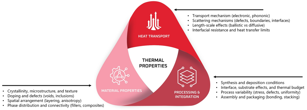
Figure 1. Thermal properties reflect the interaction of fundamental heat transport mechanisms, material structure, and processing and integration conditions. Reliable semiconductor thermal modeling requires properties representative of the actual materials, interfaces, and operating conditions, rather than relying solely on nominal bulk-material values.
This relationship helps explain why two nominally identical material stacks may exhibit different thermal behavior after changes in deposition, bonding, annealing, or other manufacturing steps. It also highlights an important distinction: a model can accurately solve the governing heat-transfer equations while still producing misleading predictions if its material inputs do not represent the manufactured structure. As Semiconductor Engineering observes: “A model can be accurate and still be wrong for the question asked.”
Measurement and Simulation Must Evolve Together
The emerging engineering challenge is not a choice between modeling and experimentation. Both are necessary, and their relationship needs to become more iterative. Simulation provides the ability to evaluate architectures, explore design alternatives, and investigate operating conditions that may be difficult or expensive to reproduce experimentally. Measurement provides the physical evidence needed to establish material inputs, calibrate assumptions, and assess whether predictions remain representative.
For advanced semiconductor systems, a measurement-driven thermal design workflow should consider several questions:
- Scale: Were thermal properties measured at thicknesses and dimensions representative of the actual device?
- Interfaces: Does the model account for thermal boundary resistance between adjacent materials?
- Directionality: Are in-plane and cross-plane thermal conductivities appropriately distinguished?
- Process variability: How do deposition, bonding, processing, and manufacturing variation affect thermal behavior?
- Operating conditions: Are temperature-dependent properties and relevant operating conditions adequately represented?
These questions become increasingly important as heat flow is controlled by localized structures and buried interfaces rather than by bulk materials alone. Measurements do not eliminate uncertainty, nor can every property be measured directly in a completed device. But they help establish which assumptions require experimental support and where a model’s predictive confidence may be limited.
The objective is not simply better thermal data. It is a stronger connection between material characterization, process development, and semiconductor design.
From Physical Measurement to Better Engineering Decisions
At Laser Thermal, this is the engineering problem our thermal metrology technologies are designed to address.
FASTR, using steady-state and frequency-domain thermoreflectance techniques, measures thermal conductivity, thermal boundary resistance, and volumetric heat capacity in thin films and multilayer material systems. These measurements can support more representative simulation inputs and help engineers investigate changes introduced by materials processing and interface formation.
For larger-scale packaging materials, TOPS provides complementary thermal conductivity and thermal resistance measurements, including characterization of thermal interface materials and other materials used in electronic assemblies.
Neither measurement technique replaces device-level thermal simulation. Instead, they help connect model assumptions to the thermal behavior of real materials. As semiconductor engineering moves thermal analysis upstream, material characterization must become part of that same early design conversation.
The next advance in thermal design may depend not only on how accurately engineers can simulate heat flow, but on how confidently they know the properties of the materials through which that heat must travel.
ARTICLES LISTED:
SEMICONDUCTOR ENGINEERING (October 28) – How Much Can Semiconductor Models Hide?
IMEC RESEARCH (featured October 27; underlying research previously published) – Beyond HBM-on-GPU: Thermal Design Envelope for 3D Volumetric DRAM-on-GPU Integration
IEEE RESEARCH (featured October 27; underlying research previously published) Self-Heating and Parasitic Effects in Multi-Tier CFET Design
KEYSIGHT (October 29) – Is it Getting Hot in Here? Why Thermal is No Longer a Signoff Problem