Our world runs on semiconductors, and chip manufacturers are always looking for improvements that can help deliver higher yield and lower costs in the fabrication process. Testing plays a vital role in identifying defective chips at each stage of the semiconductor manufacturing process to help minimize wasted processing time and maximize the opportunity for rework. Notably, for new chip designs, device architectures, and materials, testing is essential to establish the right performance specifications.
In this post, we examine the semiconductor testing process, how it works, and why it’s particularly critical for this industry. Thermal resistance measurements, particularly quantifying thermal conductivity testing and interfacial thermal resistance testing, are a crucial part of this process, and we conclude with a look at a thermal conductivity testing instrument from Laser Thermal that enables the semiconductor industry to quickly and precisely measure these critical thermal properties.

How does the semiconductor testing process work?
Fundamentally, semiconductor device testing works by generating electrical test signals which are fed into a semiconductor device. The influence of unwanted defects can be detected by comparing the output of these test signals to the expected value for a correctly functioning component (as predicted from model calculations or as measured from a control device). This testing process is important to determine both that a semiconductor device is functional, and that it is performing within intended specifications. Importantly, the properties of the materials and interfaces that comprise the device are foundational to the expected device functionality during these tests.
Semiconductor testing can be broadly divided into two phases: wafer testing and “final” or packaging testing.
Wafer Testing as Part of Thermal Conductivity Tests
After the initial wafer fabrication process is completed, semiconductor chips are subjected to electrical die sorting tests. This process begins with basic electrical tests, with important measured values including DC voltage and the operating parameters of individual chip components (i.e., resistors, capacitors, transistors, and diodes). A wafer-level test and burn-in (WLTBI) are also employed. This process, sometimes called “probe testing,” applies a precise thermal load to the wafer before utilizing hundreds of small electrical probes to test each individual die for potential early life failures.
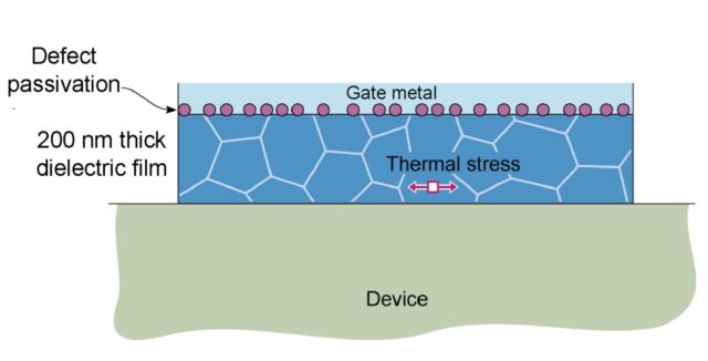
The signal testing described above is subsequently applied to categorize individual ICs on the wafer into functional/repairable and non-functional groups. At this stage, thermal property testing can also be employed to identify defects that emerge at specific operating temperatures, and thus pinpoint the critical thermal resistances that arise in the wafers due to these defects.
Repairable chips can be mended via subsequent re-lasering (followed by another round of testing). Defective chips are marked (“inked”) for discard, while functional chips proceed for further processing.
Thermal Conductivity Testing after Final Packaging
After individual chips are cut, they must be packaged in a form factor suited to their eventual application. This packaging provides protection and I/O connectivity for the circuit inside. Final packaging typically includes mounting on a printed circuit board (PCB) or lead frame, followed by encasement via an epoxy moulding compound.
Once packaging is complete, an additional round of testing can help identify subsequent defects or irregularities. This stage of testing employs a battery of voltage, burn-in, signal, and thermal testing, similar to that applied at the wafer stage.
Why Quality Testing Capabilities Are Critical for Semiconductor Manufacturers
Semiconductor manufacturing is an industry defined by ever-increasing demand and a constant quest for higher yield and throughput. In this context, more fine-tuned testing processes play an important role in improving the yield and efficiency of the semiconductor manufacturing process. The earlier and more precisely that defective chips or sub-standard materials can be identified, the more time and money can be saved.
Once identified, defective chips can be excluded from subsequent processing that costs equipment capacity, money, and labour time.
The key is identifying these defective materials, processes and chips early and as far as possible upstream in the manufacturing process.
As noted by Semiconductor Review, “replacing chips after they have been put to use is becoming challenging owing to the sophisticated designs,” placing more pressure on semiconductor manufacturers to ensure high reliability. Chipmakers are leveraging new approaches like machine learning and on-chip monitoring to identify and eliminate chronic drivers of irregularities and defects in the manufacturing process.
Our experience suggests that enhanced thermal testing capabilities are another crucial option to consider for enhancing the efficiency of semiconductor manufacturing. We explain why in the next section.

Why is it essential for semiconductor manufacturers to use thermal conductivity testing instruments?
In the testing process outlined above, thermal testing plays a key role in both initial wafer testing and testing of the final packaged IC. A key benefit of thermal testing is the ability to identify unwanted thermal resistances and defective materials early on in the manufacturing process. Due to demands on throughput, a thermal resistance measurement technique must be amenable to rapid material screening along with integration into semiconductor manufacturing cycles to achieve maximal impact. However, most traditional thermal conductivity testing instruments cannot dependably provide exact measurements of thermal resistances on the length scales needed for semiconductor chips, nor meet the integration and throughput constraints necessary for integration into the semiconductor testing market.
The inability of traditionally employed thermal metrologies to integrate into these processes are largely due to 1) the measurements are performed using contacts, requiring physical probes to be placed on each individual sample or 2) the measurement volume of the technique is too large to resolve thermal resistances on the micrometre or sub-micrometre scale.
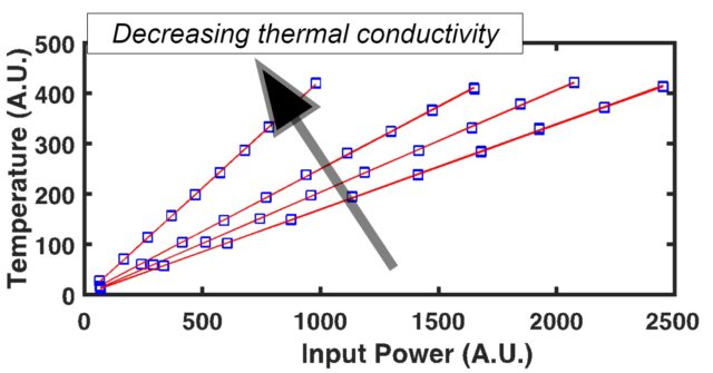
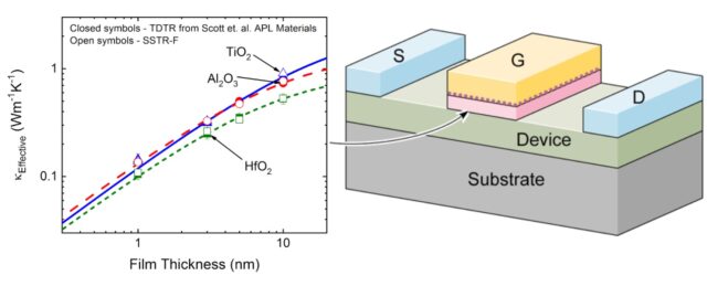
Laser Thermal’s Steady-State Thermoreflectance in Fiber Optics (SSTR-F) provides a powerful and unique thermal resistance testing metrology that overcomes the limitations of traditional approaches.
SSTR-F is thermal conductivity testing instrument that is a non-contact laser-based pump-probe technique that can measure the thermal conductivity and interfacial thermal resistance of thin films. Laser Thermal’s patented design of the SSTR-F tool allows for turnkey, fully automated thermal conductivity measurements, with high throughput batch testing that is ideal for screening thermal resistance changes in materials.
In addition to its non-contact and high throughput capabilities, SSTR-F provides accurate (+/- 10 %), repeatable (+/- 0.5 %) and reproducible (+/- 1.0 %) measurements of the thermal resistances of thin films and interfaces, offering the ideal solution to identify defects in semiconductor materials earlier and more consistently, saving time and money. For new products and materials, SSTR-F can identify exact thermal properties more quickly and accurately, helping bring products to market faster.
Learn More About Laser Thermal’s Thermal Conductivity Testing Instrument, SSTR-F, for Semiconductor Materials
If you’re interested in learning more about SSTR-F, how it works, and how it can help provide more precise thermal property measurements for challenging materials such as semiconductors, our video playlist here is a great place to start.
Or, if you have more specific questions, we encourage you to reach out to our team using the button below.